



HDI Designs
Engineered & aligned with industry best practices for PCB fabrication
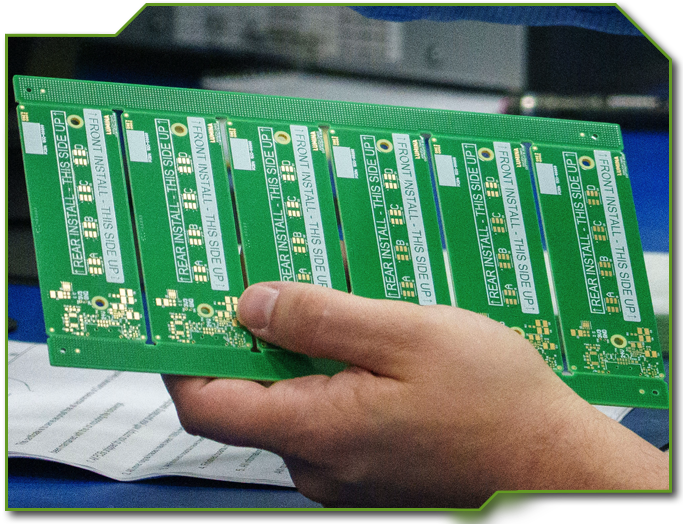
As experts in fabrication, we aim to align each program platform with relevant best practices. In doing so, we enable the highest possible yields by designing in proven constraints – enabling pathways to successful manufacturing practices. We drive DFM into cutting edge via structure design, multi-lamination definition & material selection/processing analysis.
HDI Layout Program Solutions
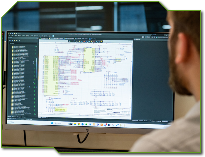
- Front-end fab-CAM interconnect strategy, stack development, via design & materials selection
- High-density layouts constrained by form factor & layer count
- Fine-pitch devices driving complex fanout & escape routing
- Signal integrity challenges across RF, high-speed digital & mixed-signal applications
- Balanced solution proposals for competing electrical, mechanical, thermal & manufacturing constraints
- Tactical layout task engagement prior to finalized schematics
- Highlighting tradeoffs between performance & manufacturability
De-Risking Supply Chain
- First-hand knowledge of material & processing limitations in fabrication
- Clear program risk communication with project stakeholders
- Early vetting & exposure of processing capability concerns in supply chain
- Early engagement ability & procurement of LLT materials to meet schedule